我们所有人都听到过警告,要确保我们在操作电子设备时正确接地,但技术的进步是否减少了静电损坏的问题,或者静电仍然像以前一样普遍?今天的超级用户问答帖子全面回答了一位好奇读者的问题。
今天的问答环节是由SuperUser提供的,SuperUser是Stack Exchange的一个分支,是一个由社区驱动的问答网站分组。
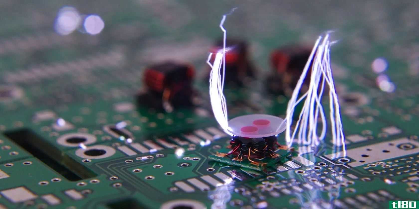
照片由Jared Tarbell(Flickr)提供。
问题
超级用户读者Ricku想知道静电损伤现在是否仍然是电子产品的一个大问题:
I have heard that static electricity was a big problem a couple of decades ago. Is it still a big problem now? I believe that it is rare for a person to “fry” a computer component now.
静电损伤现在仍然是电子产品的一个大问题吗?
答案
超级用户贡献者Argonauts为我们提供了答案:
In the industry, it is referred to as Electro-Static Discharge (ESD) and is far more of a problem now than it has ever been; although it has been mitigated somewhat by the fairly recent widespread adoption of policies and procedures that help to lower the likelihood of ESD damage to products. Regardless, its impact on the electronics industry is larger than many other entire industries.
It is also a huge topic of study and very complex, so I will just touch on a few points. If you are interested, there are numerous free sources, materials, and websites dedicated to the subject. Many people dedicate their careers to this area. Products damaged by ESD have a very real and very large impact on all the companies involved in electronics, whether it is as a manufacturer, designer, or “c***umer”, and like many things dealt with in an industry, its costs are passed along to us.
From the ESD Association:
As devices and the size of their features continuously become **aller, they become more susceptible to being damaged by ESD, which makes sense after a bit of thought. The mechanical strength of the materials used to build electronics generally goes down as their size decreases, as does the material’s ability to resist rapid temperature changes, usually referred to as thermal mass (just like in macro scale objects). Around 2003, the **allest feature sizes were in the 180 nm range and now we are rapidly approaching 10 nm.
An ESD event that 20 years ago would have been harmless could potentially destroy modern electronics. On transistors, the gate material is often the victim, but other current carrying elements can be be vaporized or melted as well. Solder on an IC’s pins (a surface mount equivalent like a Ball Grid Array are far more common these days) on a PCB can be melted, and the silicon itself has some critical characteristics (especially its dielectric value) that can be changed by high heat. Taken altogether, it can change the circuit from a semi-conductor to an always-conductor, which usually ends with a spark and a bad **ell when the chip is powered on.
Smaller feature sizes are almost entirely positive from most metrics perspectives; things like operating/clock speeds that can be supported, power c***umption, tightly coupled heat generation, etc., but the sensitivity to damage from what would otherwise be c***idered trivial amounts of energy also greatly increases as the feature size goes down.
ESD protection is built into many electronics today, but if you have 500 billion transistors in an integrated circuit, it is not a tractable problem to determine what path a static discharge will take with 100 percent certainty.
The human body is sometimes modeled (Human Body Model; HBM) as having 100 to 250 picofarads of capacitance. In that model, the voltage can get as high (depending on the source) as 25 kV (though some claim only as high as 3 kV). Using the larger numbers, the person would have an energy “charge” of approximately 150 millijoules. A fully “charged” person would not typically be aware of it and it gets discharged in a fraction of a second through the first available ground path, frequently an electronic device.
Note that these numbers assume the person is not wearing clothing capable of carrying an additional charge, which is normally the case. There are different models for calculating ESD risk and energy levels, and it gets fairly confusing very quickly since they appear to contradict each other in some cases. Here is a link to an excellent discussion of many of the standards and models.
Regardless of the specific method used to calculate it, it is not, and certainly does not sound like much energy, but it is more than sufficient to destroy a modern transistor. For context, one joule of energy is equivalent (according to Wikipedia) to the energy required to lift a medium-size tomato (100 grams) one meter vertically from the surface of the Earth.
This falls on the “worst scenario” side of a human-only ESD event, where the human is carrying a charge and discharges it into a susceptible device. A voltage that high from a relatively low amount of charge occurs when the person is very poorly grounded. A key factor in what and how much gets damaged is not actually the charge or the voltage, but the current, which in this context can be thought of as how low the resistance of the electronic device’s path to a ground is.
People working around electronics are usually grounded with wrist straps and/or grounding straps on their feet. They are not “shorts” for grounding; the resistance is sized to prevent the workers from serving as lightning rods (easily getting electrocuted). Wrist bands are typically in the 1M Ohm range, but that still allows for the quick discharging of any accumulated energy. Capacitive and insulated items along with any other charge generating or storing materials are isolated from work areas, things like polystyrene, bubble wrap, and plastic cups.
There are literally countless other materials and situati*** that can result in ESD damage (from both positive and negative relative charge differences) to a device where the human body itself does not carry the charge “internally”, but just facilitates its movement. A cartoon level example would be wearing a wool sweater and socks while walking across a carpet, then picking up or touching a metal object. That creates a significantly higher amount of energy than the body itself could store.
One last point on how little energy it takes to damage modern electronics. A 10 nm transistor (not common yet, but it will be in the next couple of years) has a gate thickness less than 6 nm, which is getting close to what they call a monolayer (a single layer of atoms).
It is a very complicated subject, and the amount of damage an ESD event can cause to a device is difficult to predict due to the huge number of variables, including the speed of discharge (how much resistance there is between the charge and a ground), the number of paths to a ground through the device, humidity and ambient temperatures, and many more. All of these variables can be plugged into various equati*** that can model the impact, but they are not terribly accurate at predicting actual damage yet, but better at framing the possible damage from an event.
In many cases, and this is very industry specific (think medical or aerospace), an ESD-induced catastrophic failure event is a far better outcome than an ESD event that passes through manufacturing and testing unnoticed. Unnoticed ESD events can create a very minor defect, or perhaps slightly worsen a pre-existing and undetected latent defect, which in both scenarios can get worse over time due to either additional minor ESD events or just regular usage.
They ultimately result in a catastrophic and premature failure of the device in an artificially shortened time frame that cannot be predicted by reliability models (which are the basis for maintenance and replacement schedules). Because of this danger, and it is easy to think of terrible situati*** (a pacemaker’s microprocessor or flight control instruments, for example), coming up with ways to test for and model latent ESD-induced defects is a major area of research right now.
For a c***umer who does not work in or know much about electronics manufacturing, it may not seem to be an issue. By the time most electronics are packaged for sale, there are numerous safeguards in place that would prevent most ESD damage. The sensitive components are physically inaccessible and more convenient paths to a ground are available (i. e. a computer chassis is tied to a ground, discharging ESD into it will almost certainly not damage the CPU inside the case, but instead take the lowest resistance path to a ground via the power supply and wall outlet power source). Alternatively, no reasonable current carrying paths are possible; many mobile phones have non-conductive exteriors and only have a ground path when being charged.
For the record, I have to go through ESD training every three months, so I could just keep going. But I think this should be sufficient to answer your question. I believe everything in this answer to be accurate, but I would strongly advise reading up on it directly to get better acquainted with the phenomenon if I have not destroyed your curiosity for good.
One thing that people find counter-intuitive is that the bags you frequently see electronics stored and shipped in (anti-static bags) are also conductive. Anti-static means that the material will not collect any meaningful charge from interacting with other materials. But in the ESD world, it is equally important (to the best extent possible) that everything has the same ground voltage reference.
Work surfaces (ESD mats), ESD bags, and other materials are all typically kept tied to a common ground, either by simply not having an insulated material between them, or more explicitly by wiring low resistance paths to a ground between all work benches; the connectors for the workers’ wrist bands, the floor, and some equipment. There are safety issues here. If you work around high explosives and electronics, your wrist band might be tied directly to a ground rather than a 1M Ohm resistor. If you work around very high voltage, you would not ground yourself at all.
Here is a quote on the costs of ESD from Cisco, which might even be a bit c***ervative, as the collateral damage from field failures for Cisco typically do not result in the loss of life, which can raise that 100x referred to by orders of magnitude:
有什么要补充的解释吗?在评论中发出声音。想从其他精通技术的Stack Exchange用户那里了解更多答案吗?在这里查看完整的讨论主题。