谁发明了intel 1103 dram芯片?
新成立的英特尔公司于1970年公开发布了1103,这是第一款DRAM(动态随机存取存储器)芯片。到1972年,它是世界上最畅销的半导体存储芯片,击败了磁芯型存储器。第一台使用1103的商用计算机是HP 9800系列。

核心存储器
杰伊·弗雷斯特(Jay Forrester)在1949年发明了核心存储器,并在20世纪50年代成为计算机存储器的主导形式。它一直使用到1970年代末。根据Philip Machanick在威特沃特斯兰德大学的一次公开演讲:
"A magnetic material can have its magnetization altered by an electric field. If the field isn't strong enough, the magnetism is unchanged. This principle makes it possible to change a single piece of magnetic material – a small doughnut called a core – wired into a grid, by passing half the current needed to change it through two wires that only intersect at that core."
单管dram
IBM Thomas J.Watson研究中心研究员Robert H.Dennard博士于1966年发明了单晶体管DRAM。丹尼纳德和他的团队正在研究早期的场效应晶体管和集成电路。当他看到另一个团队关于薄膜磁记忆的研究时,记忆芯片引起了他的注意。Dennard声称他回家后在几个小时内就得到了创建DRAM的基本想法。他在构思一种更简单的存储单元,只使用一个晶体管和一个小电容器。IBM和Dennard于1968年被授予DRAM专利。
随机存取存储器
RAM代表随机访问内存–可以随机访问或写入的内存,因此任何字节或内存段都可以在不访问其他字节或内存段的情况下使用。当时有两种基本类型的RAM:动态RAM(DRAM)和静态RAM(SRAM)。DRAM必须每秒刷新数千次。SRAM速度更快,因为它不需要刷新。
这两种类型的RAM都是易失性的–当电源关闭时,它们会丢失内容。飞兆半导体公司于1970年发明了第一款256-k SRAM芯片。最近,已经设计了几种新型的RAM芯片。
约翰·里德和英特尔1103团队
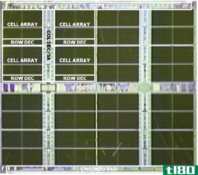
约翰·里德,现在里德公司的负责人,曾经是英特尔1103团队的一员。里德在开发英特尔1103时提供了以下存储器:
“The "invention?" In those days, Intel – or few others, for that matter – were focusing on getting patents or achieving 'inventions.' They were desperate to get new products to market and to begin reaping the profits. So let me tell you how the i1103 was born and raised.
In approximately 1969, William Regitz of Honeywell canvassed the semiconductor companies of the U.S. looking for someone to share in the development of a dynamic memory circuit based on a novel three-transistor cell which he – or one of his co-workers – had invented. This cell was a '1X, 2Y' type laid out with a 'butted' contact for connecting the pass transistor drain to the gate of the cell's current switch.
Regitz talked to many companies, but Intel got really excited about the possibilities here and decided to go ahead with a development program. Moreover, whereas Regitz had originally been proposing a 512-bit chip, Intel decided that 1,024 bits would be feasible. And so the program began. Joel Karp of Intel was the circuit designer and he worked closely with Regitz throughout the program. It culminated in actual working units, and a paper was given on this device, the i1102, at the 1970 ISSCC conference in Philadelphia.
Intel learned several lessons from the i1102, namely:
1. DRAM cells needed substrate bias. This spawned the 18-pin DIP package.
2. The 'butting' contact was a tough technological problem to solve and yields were low.
3. The 'IVG' multi-level cell strobe signal made necessary by the '1X, 2Y' cell circuitry caused the devices to have very small operating margins.
Although they continued to develop the i1102, there was a need to look at other cell techniques. Ted Hoff had earlier proposed all possible ways of wiring up three transistors in a DRAM cell, and somebody took a closer look at the '2X, 2Y' cell at this time. I think it may have been Karp and/or Leslie Vadasz – I hadn't come to Intel yet. The idea of using a 'buried contact' was applied, probably by process guru Tom Rowe, and this cell became more and more attractive. It could potentially do away with both the butting contact issue and the aforementioned multi-level signal requirement and yield a smaller cell to boot!
So Vadasz and Karp sketched out a schematic of an i1102 alternative on the sly, because this wasn't exactly a popular decision with Honeywell. They assigned the job of designing the chip to Bob Abbott sometime before I came on the scene in June 1970. He initiated the design and had it laid out. I took over the project after initial '200X' masks had been shot from the original mylar layouts. It was my job to evolve the product from there, which was no small task in itself.
It's hard to make a long story short, but the first silicon chips of the i1103 were practically non-functional until it was discovered that the overlap between the 'PRECH' clock and the 'CENABLE' clock – the famous 'Tov' parameter – was very critical due to our lack of understanding of internal cell dynamics. This discovery was made by test engineer George Staudacher. Nevertheless, understanding this weakness, I characterized the devices on hand and we drew up a data sheet.
Because of the low yields we were seeing due to the 'Tov' problem, Vadasz and I recommended to Intel management that the product wasn't ready for market. But Bob Graham, then Intel Marketing V.P., thought otherwise. He pushed for an early introduction – over our dead bodies, so to speak.
The Intel i1103 came to market in October of 1970. Demand was strong after the product introduction, and it was my job to evolve the design for better yield. I did this in stages, making improvements at every new mask generation until the 'E' revision of the masks, at which point the i1103 was yielding well and performing well. This early work of mine established a couple of things:
1. Based on my analysis of four runs of devices, the refresh time was set at two milliseconds. Binary multiples of that initial characterization are still the standard to this day.
2. I was probably the first designer to use Si-gate transistors as bootstrap capacitors. My evolving mask sets had several of these to improve performance and margins.
And that's about all I can say about the Intel 1103's 'invention.' I will say that 'getting inventions' was just not a value among us circuit designers of those days. I am personally named on 14 memory-related patents, but in those days, I'm sure I invented many more techniques in the course of getting a circuit developed and out to market without stopping to make any disclosures. The fact that Intel itself wasn't concerned about patents until 'too late' is evidenced in my own case by the four or five patents I was awarded, applied for and assigned to two years after I left the company at the end of 1971! Look at one of them, and you'll see me listed as an Intel employee!"
- 发表于 2021-09-26 00:36
- 阅读 ( 295 )
- 分类:科学
你可能感兴趣的文章
英特尔的3d堆叠lakefield芯片将在笔记本电脑、平板电脑和可折叠设备上与arm展开较量
...终于正式亮相,有望为硬件**商带来一个更小、更通用的芯片组选项,用于新的超便携、可折叠和双屏设备,这可能是英特尔迄今为止最好的ARM解决方案。 新的“采用英特尔混合技术的英特尔核心处理器”(一个几乎...
三星为下一代移动设备开发更快的dram芯片
三星宣布,它已经为移动设备开发了一款4Gb LPDDR3动态RAM芯片,该芯片的速度是前代产品的1.5倍,功耗降低20%。这些芯片采用30纳米处理技术,以每秒1600兆比特的速度传输数据,而LPDDR2的传输速率为1066兆比特,从2012年第二季度开...

存储器(sram)和德拉姆(dram)的区别
...参见弗吉尼亚大学的这一工程讲座。 动态ram(dram) DRAM芯片中的每个存储单元保存一位数据,由晶体管和电容器组成。晶体管起着开关的作用,它允许存储器芯片上的控制电路读取电容器或改变其状态,而电容器则负责保持1或0...

猛撞(ram)和存储器(sram)的区别
...元的信息行和列相交于该单元。它是由半导体材料和电子芯片制成的。这些芯片安装在小型电路板上,这些电路板安装在PC的主板上。它以动态随机存取存储器(DRAM)的形式作为计算机的主存储器。 RAM主要有两种类型—DRAM和SRAM...

墙纸综述:电路的亲密生活
...可用图像按finstr排序的节点直接链接到最大可用图像dram芯片research@intel直接链接到最大可用图像纠错芯片research@intel直接链接到最大可用图像

谁发明了地球日?
问题:谁发明了地球日? 全球180多个国家每年都庆祝地球日,但谁第一个想到地球日并开始庆祝呢?谁发明了地球日? 答:来自威斯康星州的民主党参议员盖洛德·纳尔逊(Gaylord Nelson)通常被认为是构思了美国第一个地球...

谁发明了微芯片?
一块比你的指甲还小的微芯片包含一种叫做集成电路的计算机电路。集成电路的发明历来是人类最重要的创新之一。几乎所有现代产品都使用芯片技术。 以发明微芯片技术而闻名的先驱是杰克·基尔比和罗伯特·诺伊斯。1959...

英特尔公司历史
...钱产品是3101肖特基双极64位静态随机存取存储器(SRAM)芯片。一年后的1970年,英特尔推出了1103 DRAM内存芯片。 1971年,英特尔推出了当今世界上最著名的单芯片微处理器(片上计算机)——英特尔工程师费德里科·法金(Federic...

谁发明了薯片?
据传说,土豆片是由一位鲜为人知的厨师和美国历史上最富有的人之一的口角而生的。 该事件据称发生在1853年8月24日。乔治·克拉姆(George Crum),一半是非洲裔,一半是美洲土著,当时在纽约萨拉托加泉(Saratoga Springs)的...

计算机存储器的历史
...读存储器。 1932年的今天,古斯塔夫·陶舍克在奥地利发明了鼓记忆。 1936年的今天,康拉德·祖泽申请了一项在他的计算机上使用的机械存储器专利。这种计算机内存基于滑动金属部件。 1939年的今天,赫尔穆特·施雷耶发明...
0 篇文章


